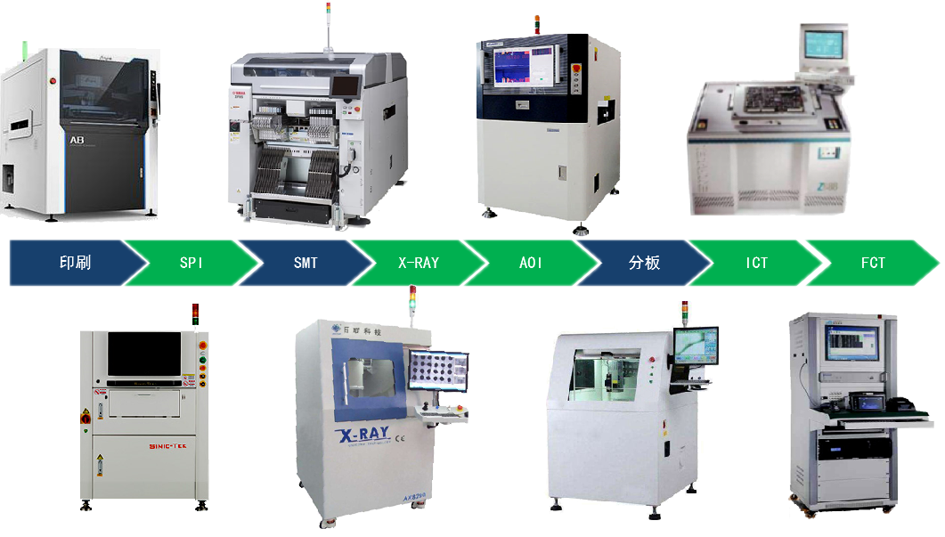
Shenzhen EuroKai Circuit Co., Ltd. is a reliable electronic contract foundry, we have been engaged in electronic processing for many years, with rich industry experience. The factory has advanced PCBA manufacturing equipment and instruments, and is committed to helping customers improve market competitiveness, shorten delivery time, improve quality, and have better cost performance. Our production is flexible, the equipment performance is superior, and we can undertake high-precision product projects such as new energy and energy storage in the industry. For product projects, Shenzhen Eurokai Circuit Co., Ltd. grasps 2 quality key points: advanced production equipment and process manufacturing capabilities.

Manufacturing Services:
♥PCBA assembly (RoHS & Reach) services
♦PCB layout services;
♦ Single and double panel PCB;
♦ Multilayer PCB with up to 16 layers;
♦RoHS, Reach, UL PCB board;
♦ Printed circuit board (PCB) hardboard/flex board manufacturing services;
♦ Laser stencil production;
♦ Sample preparation to high-volume PCB processing and manufacturing services;
♦ PCBA assembly services from sample preparation to mass production;
♦ Electrical performance testing;
♦ Selective soldering technology
♦ A small number of multi-layer high-precision and high-difficulty boards are manufactured and assembled
♥SMT patch services
♦ Capacity: 6 SMT processing lines, daily production capacity of 2 million points.
♦ Machinery and equipment:
¤1 taping machine
¤16 automatic loading machines;
¤16 automatic solder paste printing machines;
¤SPI automatic solder paste detector 6 sets
¤Mounters: 28 (14 FUJI NXTIII high-speed mounters, 6 YAMAHA high-speed mounters, 8 Samsung high-speed mounters);
¤6 reflow soldering furnaces;
¤2 sets of automatic plate packers;
¤4 sets of first article detector;
¤4 sets of online AOI detectors; 6 offline AOI detectors;
¤X-RAY8200 detector 1 set;
¤Stencil polishing machine 1, stencil cleaning machine 1 set;
¤1 oven;
¤1 PCBA board splitting machine;
¤BGA rework station 1 set;
♦ Mountable component packages:
¤01005 to 2512; QFP, QFN, CSP, TSOP, SOJ, BGA, uBGA, etc
♦ Placement Capability Parameters:
¤Number of substrate layers: 1~16 layers;
¤Substrate: FR-4, CEM-1, CEM-3, High TG, FR4 Halogen Free, FR-1, FR-2, aluminum substrate
¤Substrate thickness: 0.2~7.0mm ;
¤Maximum PCB size: 510mm X 410mm PCB minimum size: length 50 * width 50mm
¤Copper thickness: 0.5~4.0oz;
¤SMD accuracy: laser identification± 0.05mm,
¤Image recognition: ±0.03mm
¤Element height: 6mm (max.);
¤Pin pitch: laser recognition 0.65mm; High resolution VCS 0.2mm
¤Spherical spacing: laser recognition 1.0mm; High resolution VCS 0.25mm
¤BGA sphere distance: ≥0.25mm;
¤BGA spherical pitch: ≥0.25mm;
¤BGA ball diameter: ≥0.1mm;
¤IC foot pitch: ≥0.2mm
♦ Quality control:
¤The first article must be inspected for each changeover
¤100% AOI test, X-Ray test, functional test before shipment, to ensure that there are no defective products leaving the factory


